How Are Multi-Layer PCBs Manufactured?
Multi-layer PCBs are the backbone of modern electronics, enabling complex circuits in compact designs. Understanding the manufacturing process of these intricate boards reveals the advanced techniques and materials that ensure reliability and performance. This article delves into the step-by-step journey of multi-layer PCB production, highlighting its significance across various industries and the quality assurance methods that uphold high standards. For comprehensive PCB assembly services in the USA, OurPCB provides exceptional expertise and quality. More details can be found at https://www.ourpcb.com/pcb-assembly/usa.
Overview of Multi Layer PCBs
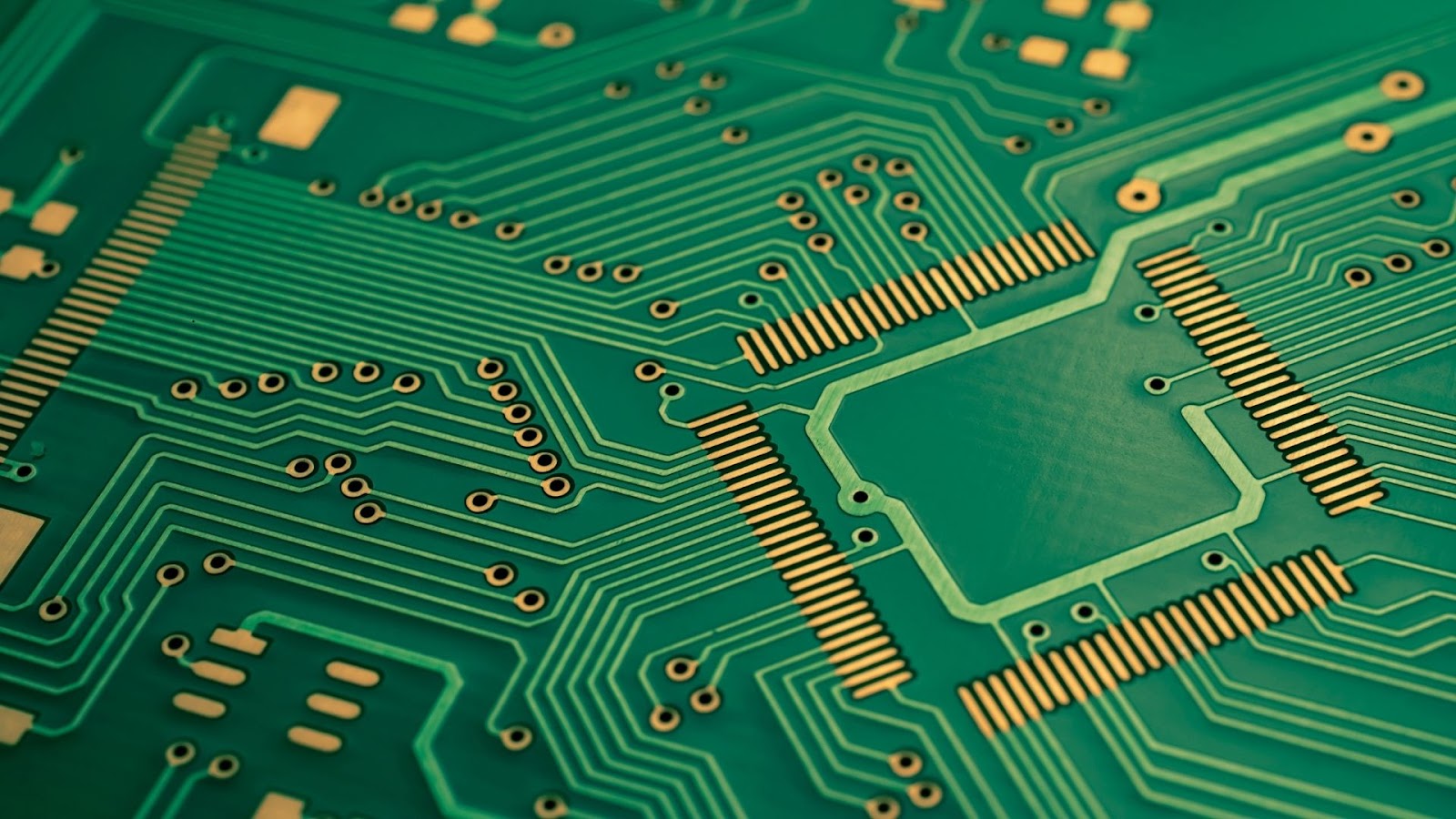
Multi-layer printed circuit boards (PCBs) consist of multiple layers of conductive and insulating materials. Each layer carries electrical signals and helps manage power distribution, making multi-layer PCBs essential for modern electronic devices.
The manufacturing process involves several critical steps:
Design: The design phase utilizes software such as Eagle, Proteus, Altium, or KiCAD to create the PCB layout. This design dictates how each layer will be arranged and interconnected.
Inner Layer Core: The process begins with creating the inner layer core, which is coated with a thin layer of copper on both sides. This core serves as the foundation for subsequent layers.
Lamination: The inner layer core undergoes lamination, where prepreg sheets and copper foil sheets are layered. A heated hydraulic press applies pressure, heat, and vacuum to ensure proper bonding without air pockets.
Curing: During curing, the resins from the prepregs bind together the core and foil layers. This step solidifies the structure, forming a durable multilayer PCB.
Layer Arrangement: The arrangement of layers includes dedicated ground and power planes. Such configurations optimize signal transmission while minimizing electrical noise.
Manufacturers can produce multi-layer PCBs with up to 50 layers, accommodating various thicknesses from 0.1mm to 10mm. Advanced inspection methods, including Automated Optical Inspection (AOI) and X-Ray Inspection, ensure quality at each stage of production. These techniques detect defects and verify solder joint integrity, ensuring reliable performance in the final application.
Multi-layer PCBs find applications in telecommunications, automotive systems, medical devices, and consumer electronics. Their reliability and performance make them vital components in today's electronic products.
Material Selection
Material selection plays a critical role in the manufacturing of multi-layer printed circuit boards (PCBs). The chosen materials significantly influence the performance, durability, and reliability of the final product.
Types of Materials Used
FR4 (Flame Retardant 4): FR4 serves as the most widely used material for PCBs due to its balanced cost, performance, and durability. This glass and epoxy resin composite withstands standard operating conditions effectively.
High-Temperature Materials: High-temperature materials, including polyimide and ceramic, excel in applications that require enhanced reliability under extreme thermal conditions. These materials can endure elevated temperatures and harsh environments, making them ideal for specialty PCBs.
Flexible Materials: Flexible materials, such as polyimide, allow for bendable PCB designs that suit applications where space-saving and flexibility are paramount. These materials adapt easily to various shapes and configurations.
Importance of Material Properties
Material properties directly affect the board's electrical performance and thermal management. Key attributes include:
Dielectric Constant: A lower dielectric constant enhances signal integrity, essential for high-frequency applications.
Thermal Conductivity: This property determines the rate of heat dissipation, crucial for maintaining performance and preventing failures.
Mechanical Strength: High mechanical strength ensures resistance to vibrations and physical stress, enhancing the board's lifespan.
Flame Retardance: Flame-retardant materials significantly improve safety by minimizing fire risks during operation.
Understanding these material properties and types facilitates optimal performance of multi-layer PCBs in various industries, such as telecommunications, automotive systems, medical devices, and consumer electronics.
Manufacturing Process
The manufacturing process of multi-layer PCBs involves several critical stages that ensure the final product meets stringent performance standards. Below are key steps in the process.
Design and Layout
The design and layout of multi-layer PCBs form the foundation of their performance. This stage includes overall requirement analysis, where the application's needs dictate design parameters. Schematic diagram designing follows, mapping out electrical connections. Component selection involves identifying suitable parts based on specifications. Layer count and sequence specifications determine the number of layers and their arrangement. Component placement maximizes space and optimizes signal paths. The routing process connects components, while signal integrity analysis identifies potential issues to improve performance. Proper heat dissipation strategies prevent overheating, and DFM checks ensure manufacturability. A thorough, complete design review finalizes the layout.
Layer Stacking
Layer stacking establishes the physical configuration of multi-layer PCBs. This step involves arranging different material layers in a specific order based on functional requirements. The core layer, often made from FR4, provides structural integrity. Additional layers may include signal, ground, and power connections. Each layer contributes to the overall functionality and performance of the PCB. Proper alignment during stacking is crucial for minimizing defects.
Etching and Drilling
Etching and drilling create the desired circuit patterns on the PCB layers. In the etching process, a photoresist layer is applied to protect specific areas of the copper layer. Exposing the photoresist to UV light forms a pattern, and the unprotected areas are subsequently etched away, revealing the desired circuitry. Drilling follows, where precision drills create holes for vias and component pins. This stage ensures connectivity between layers.
Laminating Layers
Laminating layers binds the stacked layers together, providing rigidity and stability. This process typically involves heat and pressure, activating the adhesive properties of the prepreg material used between layers. After laminating, the PCB undergoes a cooling period to solidify the structure. The result is a robust multi-layer PCB that can withstand operational stresses and fulfill electrical specifications.
Testing and Quality Control
Testing and quality control are vital in the manufacturing of multi-layer PCBs to ensure performance and reliability. Rigorous testing procedures help identify defects and confirm that the product meets industry standards.
Methods of Testing
Visual Inspection: Personnel check for visible defects, such as misaligned layers or incomplete etching, using magnifying tools.
Electrical Testing: Techniques like in-circuit testing and flying probe testing assess conductive paths and verify the operational integrity of circuits.
Functional Testing: Devices undergo simulation of operational environments to ensure that they function correctly under intended use conditions.
X-ray Inspection: Advanced X-ray technology detects internal defects, such as via bridging or insufficient connections, which are not visible externally.
Thermal Testing: Thermographic cameras evaluate heat distribution across the PCB, identifying hotspots that may affect performance or lifespan.
Importance of Quality Assurance
Quality assurance ensures the reliability and longevity of multi-layer PCBs. It reduces the risk of failures that could lead to costly recalls or product malfunctions. Stringent quality assurance processes encompass:
Standard Compliance: Adhering to international standards, such as IPC-A-600 and IPC-6012, guarantees that PCBs meet specific requirements for quality.
Process Control: Implementing control measures throughout manufacturing minimizes variation, enhancing product consistency.
Traceability: Maintaining accurate records of materials and processes allows manufacturers to trace any issues back to their source, facilitating resolution.
Customer Confidence: Delivering high-quality products fosters trust in manufacturers, leading to increased customer satisfaction and repeat business.
These methods and quality assurance practices ensure that multi-layer PCBs perform optimally in demanding applications, meeting the rigorous standards of modern electronics.
Advantages and Applications of Multi Layer PCBs
Multi-layer PCBs offer several advantages that improve their usability across various sectors.
High Density: Multi-layer PCBs accommodate a larger number of connections, making them suitable for compact electronic devices with tight space constraints.
Improved Performance: Their design minimizes signal interference and enhances electrical performance. This feature is crucial for high-frequency applications, contributing to efficient signal transmission.
Thermal Management: Multi-layer PCBs can dissipate heat more effectively. This capability is vital in applications where components generate significant heat, such as automotive electronics.
Durability: Constructed with high-quality materials, multi-layer PCBs withstand harsh environments. They excel in industries requiring reliable and long-lasting performance, such as telecommunications and medical devices.
Design Flexibility: Their modular structure allows for intricate designs, accommodating complex circuitry and component arrangements. This flexibility meets the demands of innovative product designs.
Telecommunications: Multi-layer PCBs serve as the backbone of communication devices, providing reliability and performance for signal transmission.
Automotive: Multi-layer PCBs are essential for automotive electronics, ensuring they perform well under varying temperatures and conditions.
Medical Devices: Used in medical instrumentation, multi-layer PCBs support high precision and stringent quality standards, crucial for patient safety.
Consumer Electronics: Multi-layer PCBs are prevalent in consumer products, offering cost-effective solutions without compromising performance.
Aerospace: Multi-layer PCBs help meet the strict requirements of aerospace applications, providing durability and reliability in critical systems.
Frequently Asked Questions
What are multi-layer PCBs?
Multi-layer printed circuit boards (PCBs) are electronic boards that have multiple layers of circuitry. They enable higher circuit density and improved performance, making them essential for complex electronic devices.
Why are multi-layer PCBs important?
Multi-layer PCBs are crucial because they optimize space and allow for advanced thermal management. Their durability and design flexibility improve reliability in various applications, including telecommunications and medical devices.
How are multi-layer PCBs manufactured?
The manufacturing process of multi-layer PCBs involves several steps: design, layer stacking, lamination, drilling, plating, and finally, testing for quality assurance. This ensures a robust final product.