 SB600
- CP1 Improvements
SB600
- CP1 Improvements
 (user friendly)
SB600
- CP1 Improvements
(user friendly)
|
|
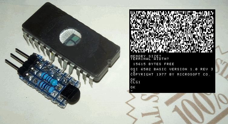
SB600/C1P/UK101 adding SD card option Usually, a SB600 does not offer any mass storage option without a 610 floppy disk interface board together with external floppy disk drives. If you own a SB600/C1P or UK101 in a basic 4K or 8K RAM configuration, you are left with the build in 300 baud cassette/serial interface. Loading an 8k game can take easily 14 minutes to load. The idea was to crate a easy plug and play module, that does not require any modification to the machine, can interface to a regular FAT formatted SD card and provides the same cassette/serial interface function as before. As the serial communication is managed by an Motorola MC6850P ACIA chip, that is conveniently socketed in all the lower spec OSI boards. Why not replace the ACIA by a software defined MC6850P including a SD card interface ? That said, here my plug and play module I came up with and its basic functionality: Shown the board plugged into the ACIA socket and ribbon cable attached to a simple SD card interface
Main functions: -
board emulates 6850P ACIA functions for systems with up to 1Mhz
clocked CPU
|
|
SMD version details
DIP version details
|
|
|
|
THE SUPERBOARD LIMITATIONS SB600/C1P adding graphic capabilities Beside some
graphic characters a SB600 does not offer any graphic mode beside
the ordinary text screen. You can get up to 128x128 pixel for an updated C1P with 64x32 characters or 128x64 pixel on a standard SB600 that can be individually set or cleared, like in an additional graphic mode. The graphic section will be on top of the screen (Half screen) or can be set to Full screen. For gaming, the best option is to use the half screen mode, so you can display text at the bottom and do all graphic visualizations on the top.
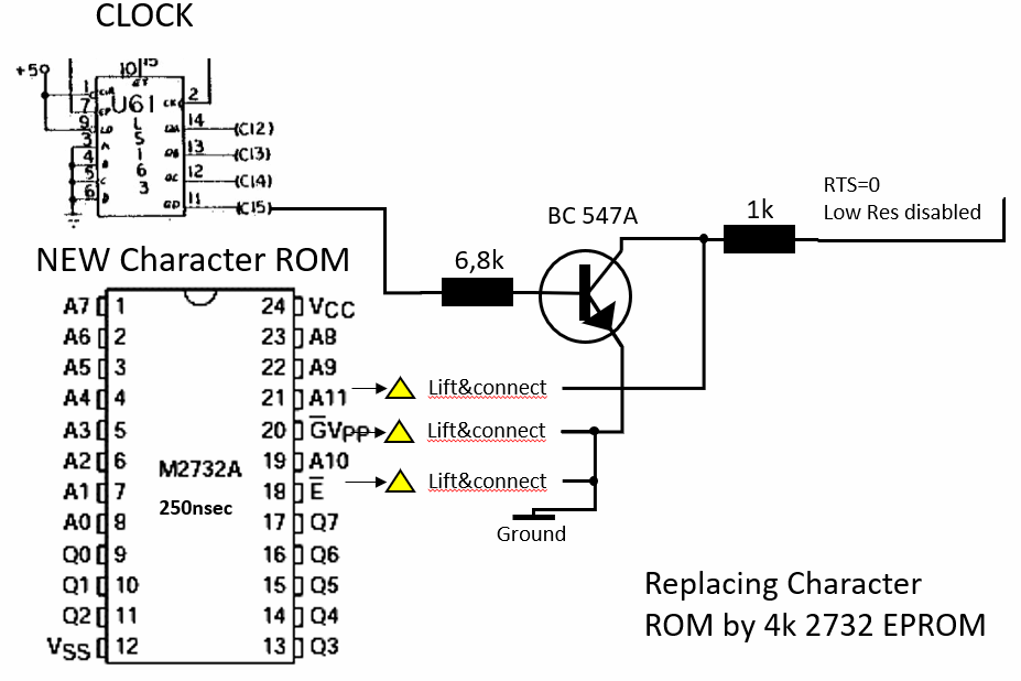
The idea is to replace the socketed Character ROM by an 4k (2732) Eprom with a bitmap scheme in the second half of the Memory. It is possible to enable or disable the bitmap section by Software, when connected to the RTS line of the ACIA6850. Two versions of Character ROMS a available (4x2 type and 2x4 type) with different characteristics concerning horizontal and vertical resolution. See the following options: Unmodified SB600 with 32x32 screen (1k video memory) Half screen: 128x32 with CHARGEN_LRES4x2.ROM Full screen: 128x64
Unmodified UK101 with 64x16 screen (1k video memory) Half screen: 256x16 with CHARGEN_LRES4x2.ROM Full screen: 256x32
Modified SB600/C1P with 64x32 screen (2k video memory) Half screen: 256x32 with CHARGEN_LRES4x2.ROM Full screen: 256x64
Unmodified SB600 with 32x32 screen (1k video memory) Half screen: 64x64 with CHARGEN_LRES2x4.ROM Full screen: 64x128
Unmodified UK101 with 64x16 screen (1k video memory) Half screen: 128x32 with CHARGEN_LRES2x4.ROM Full screen: 128x64
Modified SB600/C1P with 64x32 screen (2k video memory) Half screen: 128x64 with CHARGEN_LRES2x4.ROM Full screen: 128x128 The
shown 2732 EPROM is connected to a small prototype
PCB. Connector pins have to be connected to:
See attached PDF guide for reference. |
|
ROMS |
|
|
|
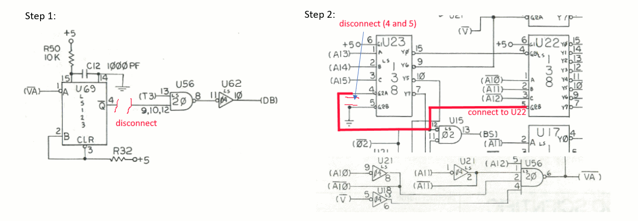
SB600 Revision B flicker fix When using a SB600 connected to a monochrome monitor, the first thing you may notice are white artifacts on the screen when scrolling or printing characters. This is one of the limitations that was improved in later Revisions of the board. During access to the Video memory (VA), a display blank (DB) signal is generated. This blanks out the video pixel stream from the U42 shift register (see U70 pin 1). For example, during text scrolling, you may have observed that characters are partially blanked and the whole screen seems annoyingly to flicker. The more access the video memory gets, the more flicker is visible.
Reason for this behavior is the fact, that the VA encoder uses only address lines, so that VA is active over more that 2/3 of the CPU clock cycle. Also the CPU clock signal (Q0 and Q2) are synchro to the C0 counter and therefore the Latch signal generated by U19 (see above) The modification will invert Q0/Q2 to C0 and eliminate the blacking signal DB going to U70.
Starting with U69 (placed nearby the video connector). I most cases, this IC is socketed on most boards. In case U69 is in a socked, lift the IC carefully out and bend pin 4 slightly to the outside. When placing the IC back, make sure the pin stays outside the socket connector. In case U69 is soldered to the board, you have to cut the trace coming out of pin 4. In the next step, we have to modify VA,
so that is only valid during the active Q2 clock phase. VA is driven by V and
several address lines. Finally, we have to inverse the Q0 input of the CPU compared to C0. To do this, we have to use an unused 7404 inverter on the board located in U18. Pin 9 is input and pin 8 output of the inverter. The CPU Q0 clock signal is coming form
pin 14 of U30 nearby.
|
|
|
|
![]()
Last Update: May 2025